xTool S1 and PCB
07.02.26
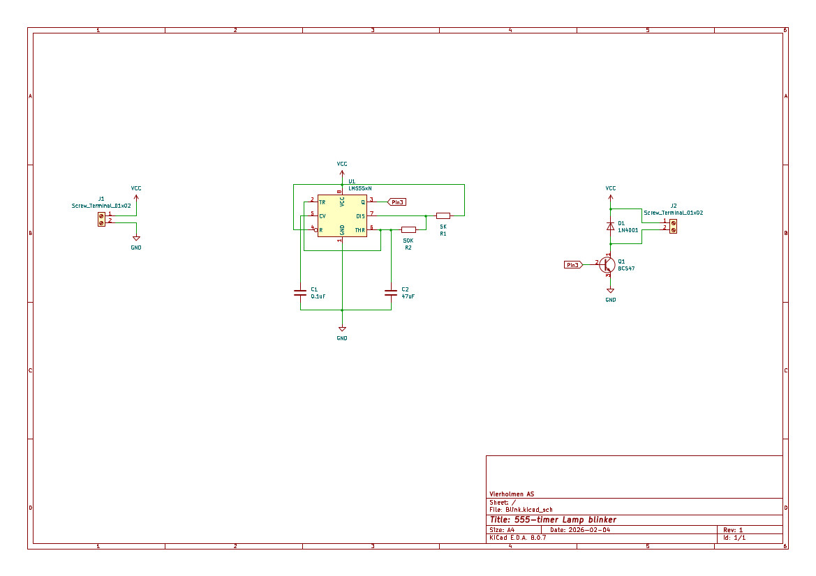
Circuits
Steps to follow to make PCB
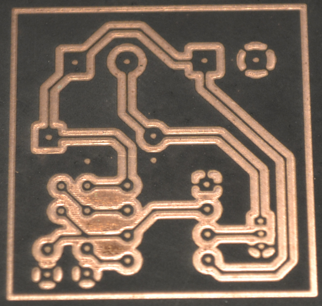
We're not etching a PCB with the xTool laser, but we're transfering the design. Start by cleaning the copper clad board thoroughly with aceton. Then apply a thin layer with acrylic paint. I'm using an airbrush.
These are the steps:
Design the PCB in your favourite eCAD software. I'm using KiCAD
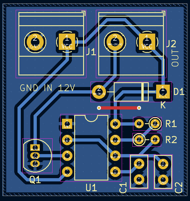
Click on image to enlarge.
The board design.
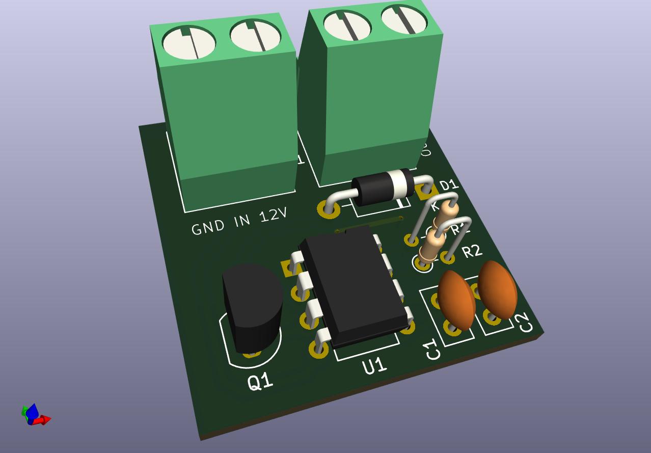
3D view - a nice feature in KiAD
Print the board with these settings:
Include layers: B.CU, Edge.Cuts.
Outputmode: Black and white
Drill marks: Small mark.
Check Print mirrored. (Bottom copper => Mirrored.)
Scale 1:1
Print to a PDF - file.
Import board in Gimp.
File=>Open=>your pdf
Open Pages as Image.
Click Image => Crop to Content.
Click Colours => Invert
Export as... and export the file.
Import the PDF image in xTool Studio.
xTool S1 settings:
Power: 30%.
Speed: 250mm/s.
Pass: 1.
Bitmap mode: Grayscale.
Lines pr cm: 300.
Engraving mode: Bi-directional.
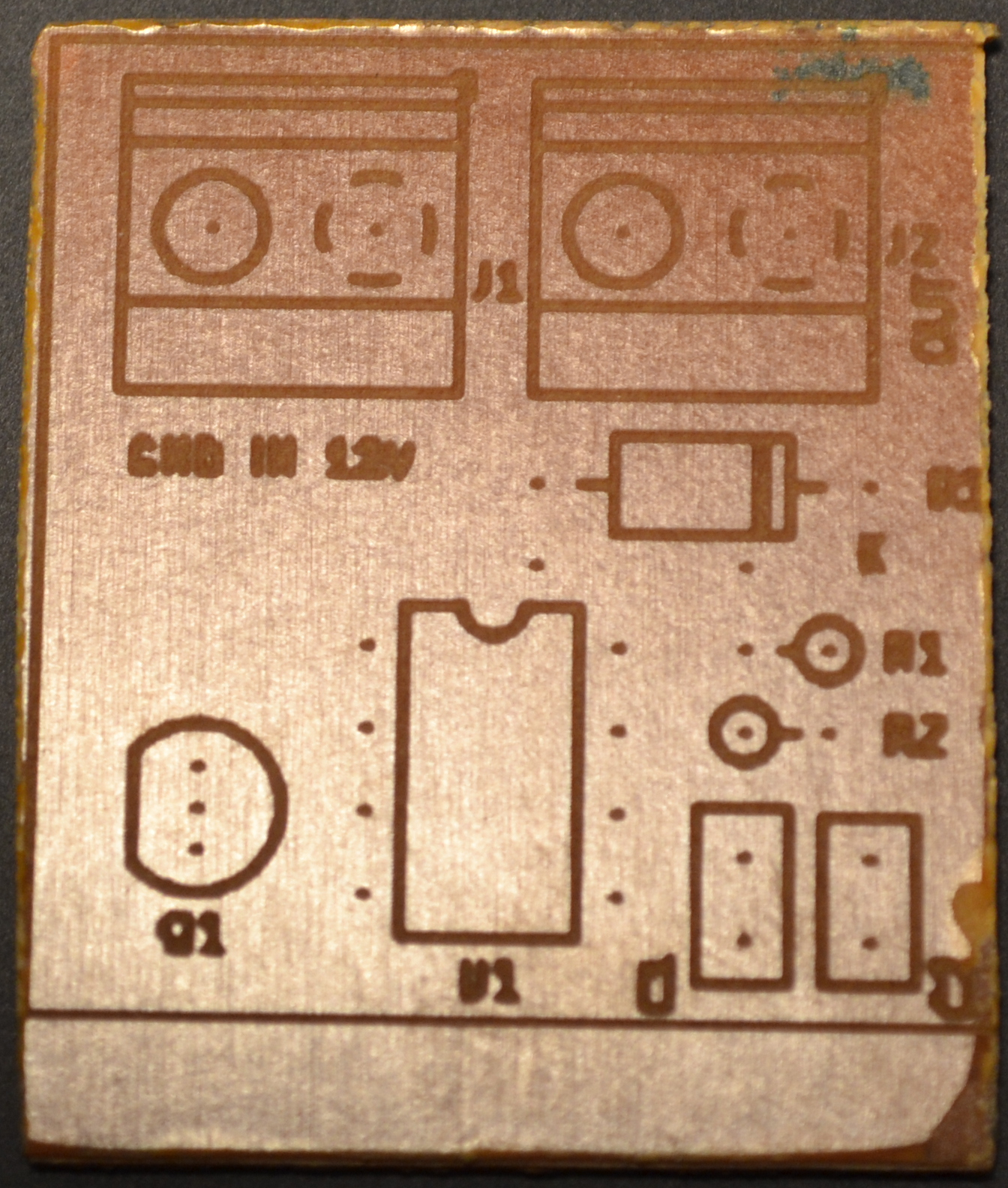
After laser engraving.
Now it's time for the Silkscreen.
Print these layers:
F.Silkscreen.
Edge.Cuts.
Black and white.
Scale: 1:1.
This is the top layer, so it must not be printed mirrored.
xTool settings for the F.Silkscreen.
Power: 25%.
Speed: 250 mm/s.
Pass: 1.
Bitmap mode: Greyscale.
Lines pr cm: 180.
Engraving mode: Bi-directional.
Back